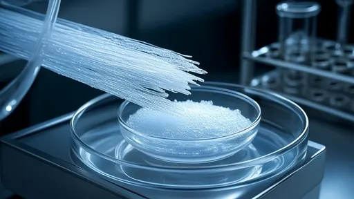
The semiconductor industry has long grappled with the challenge of silicon wafer waste management, but a groundbreaking new coloration process is turning this environmental liability into an opportunity for innovation. Researchers at the Fraunhofer Institute for Silicon Technology have developed a novel method to transform discarded silicon wafers into vibrant, functional materials through controlled oxidation and thin-film interference techniques.
From industrial byproduct to engineered material
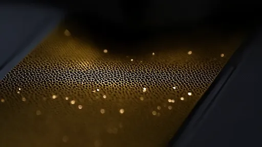
What was once considered worthless scrap now shimmers with iridescent hues under the new treatment process. The technique involves precisely controlling the oxidation parameters to grow silicon dioxide layers of specific thicknesses on waste wafers. When light interacts with these thin films, constructive interference creates intense colors ranging from deep blues to golden yellows, depending on the oxide layer's thickness. This phenomenon, similar to what makes soap bubbles appear colorful, has been harnessed to give discarded silicon a second life.
The process begins with sorting wafer fragments by crystal orientation and doping type, as these factors influence the oxidation characteristics. The fragments then undergo a modified thermal oxidation process where temperature, atmosphere, and duration are carefully controlled to achieve the desired optical properties. Unlike standard oxidation processes aimed at creating uniform dielectric layers, this method intentionally creates thickness variations to produce patterned color effects.
Beyond aesthetics: functional applications emerge
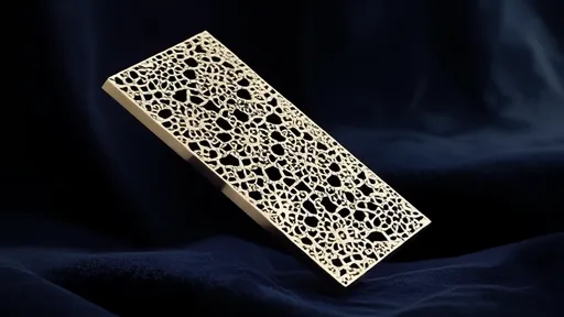
While the visual transformation is striking, the real value lies in the material's new functional properties. The colored wafers demonstrate unique light-interaction characteristics that make them suitable for specialized optical applications. Researchers have successfully incorporated the processed material into decorative architectural elements, anti-counterfeiting features for high-value components, and even as calibration standards for optical inspection systems.
One particularly promising application is in photovoltaic systems. The colored silicon exhibits modified light absorption properties that could lead to more efficient solar energy harvesting when used in certain configurations. Early tests show that some color variants actually enhance near-infrared absorption while reducing reflection losses - a potentially valuable trait for next-generation solar cells.
The environmental calculus
From an ecological perspective, the new process represents a significant improvement over traditional recycling methods. Conventional silicon recycling typically involves energy-intensive remelting processes that often degrade the material's purity. The coloration technique, by contrast, consumes relatively little energy and preserves the wafer's structural integrity. Industry analysts estimate that widespread adoption could divert thousands of metric tons of silicon waste from landfills annually.
Perhaps most importantly, the process creates economic value where none previously existed. Waste wafers that would have incurred disposal costs can now be transformed into premium-priced specialty materials. Several major semiconductor manufacturers have already begun pilot programs to implement the technology in their production facilities, seeing it as both an environmental responsibility initiative and a potential new revenue stream.
The development team continues to refine the process, working to expand the color palette and improve consistency across different wafer types. They're also investigating methods to apply the technique to other semiconductor materials beyond silicon. As the electronics industry faces increasing pressure to improve its sustainability profile, innovations like wafer coloration demonstrate how environmental challenges can spark creative technical solutions with commercial potential.
Looking ahead, researchers anticipate broader applications in consumer electronics, where colored semiconductor materials could enable new design possibilities for visible components. The automotive industry has also expressed interest in using the material for specialized sensors and decorative trim elements in high-end vehicles. What began as an experiment in waste valorization may well become a standard process in multiple industries, proving that one company's scrap can indeed become another's treasure.

By /Oct 22, 2025

By /Jul 25, 2025

By /Jul 25, 2025

By /Jul 25, 2025

By /Jul 25, 2025

By /Jul 25, 2025
By /Jul 25, 2025

By /Jul 25, 2025

By /Jul 25, 2025

By /Jul 25, 2025

By /Jul 25, 2025
By /Jul 25, 2025

By /Jul 25, 2025
By /Jul 25, 2025

By /Jul 25, 2025

By /Jul 25, 2025

By /Jul 25, 2025

By /Jul 25, 2025
By /Jul 25, 2025
By /Jul 25, 2025